Iranian Firm Produces Advanced Measuring, Optical Equipment
Among the company's flagship products are a digital camera for transmission electron microscopes (TEM), a thin film thickness gauge, and an optical surface profiler.
The thin film thickness gauge based on Fresnel diffraction technology is capable of measuring the thickness of layers with an accuracy of two nanometers. The device is about a quarter of the price of foreign models and provides results in a fraction of a second without the need for special laboratory conditions. The simple design and easy-to-use interface make it possible for non-specialized operators to use it.
The optical surface profiler is another achievement of the company which uses interferometry technology to map surfaces with an accuracy of five nanometers and dimensions of up to one square millimeter. The device is used in industries like rubber manufacturing, dentistry, and even the food industry, and is cheaper than similar foreign equipment.
In the field of structural health, the company has developed a remote vibrometer; a tool that measures the vibrations of bridges, buildings, and engines with high precision by analyzing optical patterns, and plays a key role in predicting failures and monitoring the condition of equipment.
The company has also installed special imaging cameras on these devices in recent years with the aim of digitizing transmission electron microscopes.
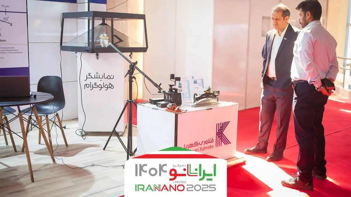
The 16th International Nano Technology Exhibition and the First Exhibition of Advanced Technologies of Iran was inaugurated at the Tehran International Fairground.
Held from November 2 to 5, the Nano Exhibition featured over 150 innovative companies showcasing advancements in nanotechnology. Meanwhile, the Exhibition of Advanced Technologies hosted 80 knowledge-based and technological products, attracting visitors, particularly students, researchers, and investors.
In a relevant development in December, an Iranian knowledge-based company stationed at Pardis Science and Technology Park had also managed to produce an atomic force microscope which is used to image and characterize samples at the nanoscale.
“One of our knowledge-based products is the atomic force microscope, which is used to image and characterize samples at the nanoscale. This device uses a sharp-pointed probe to scan the sample surface. During the scanning operation, laser light is emitted to the back of the cantilever and its reflection on a photodiode will result in the formation of an image of the sample surface,” said Seyed Abbas Shahmoradi, the managing director of the knowledge-based company.
He mentioned the Bio-AFM as another achievement of his company, and said, "This microscope is one of the most important tools for studying samples in biology, because Bio-AFM provides a suitable platform for integrating atomic force microscopy and optical microscopy in biological research projects."
Noting that the Bio-AFM microscope can capture images in different environments with diverse working modes, Shahmoradi said, “This capability allows scientists to study the structure and properties of living cells and other biological samples like DNA and RNA, proteins, viruses, bacteria, and tissues."
“Also, the Transmission Electron Microscopy (TEM) produced by our company, with an accuracy of 0.6 nanometers, is capable of providing images with extremely high resolution. For comparison, the size of the coronavirus is 120 nanometers, while the accuracy of our device is one two-hundredth of this value,” he added.
4155/v


