Iran-Made Nanoprofilometer Used in Turkish Universities

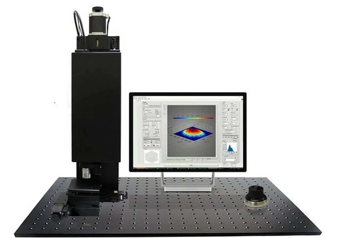
“At present, we produce 3D optical profilometer with nanometer accuracy (nanoprofilometer) and micrometer accuracy (microprofilometer). The nanoprofilometer version has been completely commercialized and is used in centers like Zanjan University and Gazi University in Türkiye,” said Solmaz Bigdeli, the commercial manager of the Iranian company.
Noting that the microprofilometer device is in the stage of making the prototype, she said, “The equipment is used for surface characterization, and they are capable of both imaging the surface and performing the necessary measurements.”
“These devices are highly useful for industries that require high precision in surface inspection. For instance, part makers or implant manufacturers are among the customers of this technology. In general, wherever a very smooth surface is needed and surface polishing is important to the manufacturer, like the production of bearings, micro and nano profilometers are needed,” Bigdeli added.
Profilometry is a technique used to extract topographical data from a surface. This can be a single point, a line scan or even a full three dimensional scan. The purpose of profilometry is to get surface morphology, step heights and surface roughness. This can be done using a physical probe or by using light.
Metrology is the science of measurement. How rough is the sample? How high are the features? How much of the area has voids or particles? What is the defect density? Answers to these questions are often quantified using profilometry.
All profilometers consist of at least two parts – a detector and a sample stage. The detector is what determines where the points on the sample are and the sample stage is what holds the sample. In some systems, the sample stage moves to allow for measurement, in others the detector moves and in some both move.
4155/v


